Power amplifier design
I’m helping put together a Faraday rotation experiment for the undergraduate physics lab. Normally these experiments are bought from companies like TeachSpin, and this is no different, however there is a missing component, the power amplifier! Due to the high levels of noise, the solenoid is driven with an AC current and a lock-in amplifier is used to take measurements (more on lock-in amplifiers here ). All this means is I need to design (or more like put together) a power amplifier that can output at least 1A pk-pk while driving the solenoid.
Requirements
Since this power amplifier is intended to replace the one from TeachSpin, there are a number of parameters that must be met
| Name | Symbol | Value |
|---|---|---|
| peak to peak current | \(I_{p-p}\) | 1 A |
| Inductance | \(L\) | 30mH |
| Inductor ESR | \(ESR_L\) | \(10\Omega\) |
| Input voltage peak-peak | \(V_{in, p-p}\) | 4 V |
Design
Current through inductors
First we need to know how much current can be pushed through the inductor, and that needs some math. Starting with the inductor I-V relationship, written as
\begin{align} V=L\frac{di(t)}{dt} \end{align}
where \(V(t)\) is the voltage, \(L\) is the inductance, and \(i(t)\) is the current. The voltage is driven by a sin wave \(V(t) = V_{p-p}\sin(\omega t)\) so we can calculate the current through the inductor as
\begin{align}
i(t)&=\int \frac{V}{L}dt \\
&=\frac{V_{p-p}}{L}\int\sin(\omega t)dt \\
&=-\frac{V_{p-p}}{L\omega}\cos(\omega t)
\end{align}
So we see that the current through the inductor is still a sinusoidal function shifted by 90 degrees. The period can be converted to frequency as \(\omega=2\pi f\), so we see that increasing either frequency or inductance will decrease the current amplitude, while increasing the maximum voltage will increase the amplitude. We know that the OPA544 has a supply range of approximately \(V_{p-p}=60V\). Using the inductance and current constraints we find the peak frequency to be
\begin{align}
f_{max}&=\frac{V_{p-p}}{2L\pi i_{max}} \\
&=\frac{60}{2\cdot0.030\cdot\pi\cdot1} \\
&\approx318Hz
\end{align}
So we have the maximum frequency of 318Hz. Of course this freqency can be increased with the use of a smaller inductor, but that will just be a bonus, here in the worst case for inductance the maximum frequency is still acceptable.
Amplifier design
For this project we are using the OPA544 since it is both in stock and in a TO-220 package. The package has a pin spacing >100mil so it won’t fit onto a standard bread board without some pin bending, but that shouldn’t affect performance. In the future the design will be put onto a PCB with a surface mount package so it can use the PCB as a heat sink (and take advantage of shorter traces), but for now we just need a working circuit.
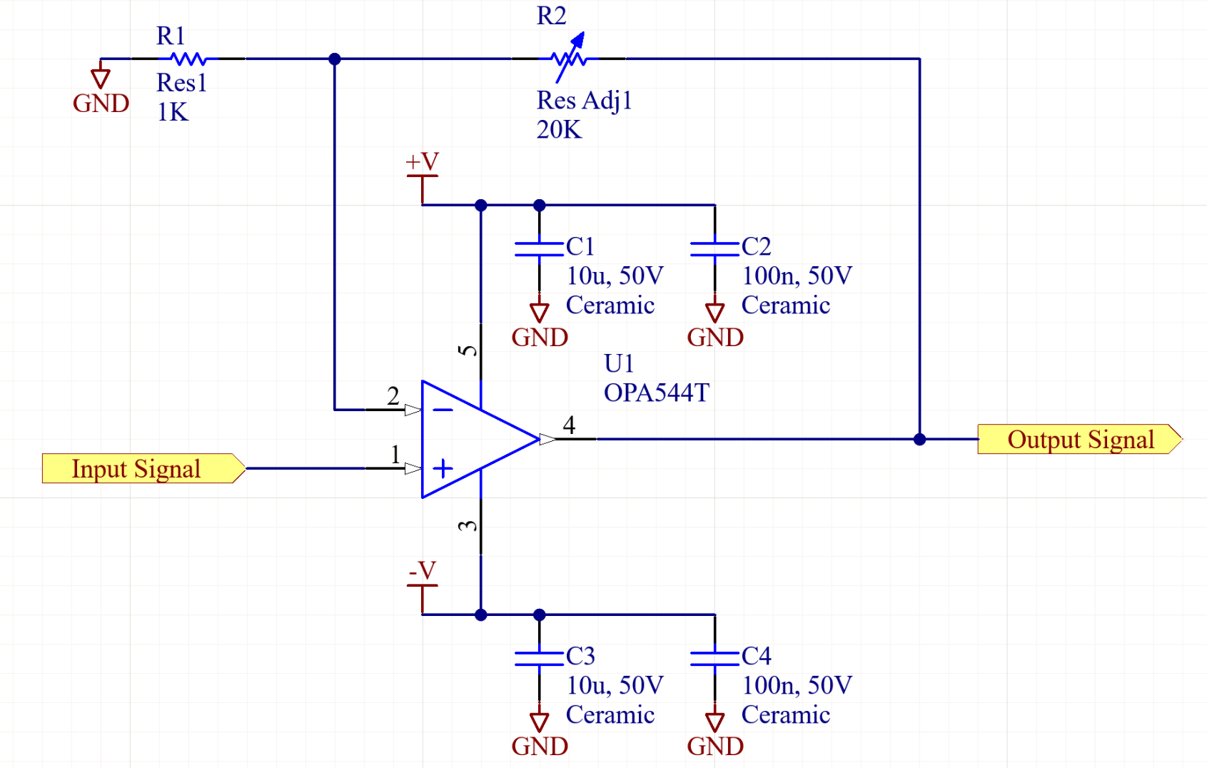
Figure 1: Basic inverting amplifier with OPA544.
For this application the OPA544 will be used in a basic non-inverting configuration shown in Figure 1 . We want to boost a \(4 V_{p-p}\) signal to \(60V_{p-p}\) which requires a maximum gain of 15. To improve flexibility we will design for a maximum gain of 20. The minimum gain should be 1 if the op amp is stable in unity gain, however it is not clear in the data sheet whether that is the case so this will be determined during testing. In the non-inverting configuration the gain is
\begin{align} G=1+\frac{R_2}{R_1} \end{align}
So by using an adjustable 20k resistor (or more likely a potentiometer) for R2, and a 1K resistor for R1 we get a maximum gain of 21 and a minimum gain of 1. This is a good starting point, but a few modifications can be made. First, if the inductor were suddenly shorted, or if the ground side had a quick change in voltage, this could cause a voltage spike at the op amp input exceeding it’s maximum ratings. To avoid this two diodes can be used to clamp the output between the positive and negative voltage rails (plus or minus the diode forward voltage). Additionally when driving inductive loads it is a good idea to add a snubber network on the output to help improve the op amp’s stability. Both of these changes can be seen in Figure 2 . Note that the values for the snubber network are subject to change during testing.
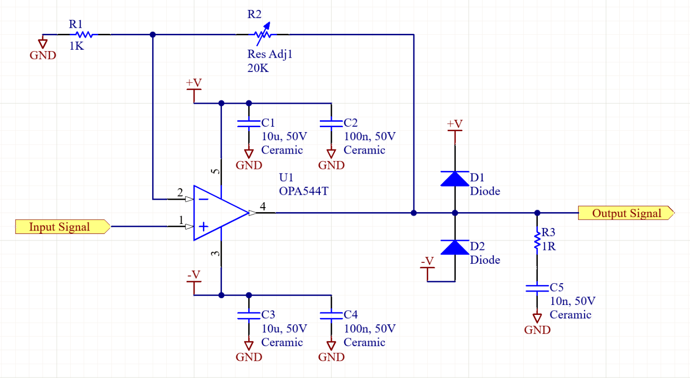
Figure 2: Basic inverting amplifier with OPA544.
Thermal considerations
Up until now we haven’t considered how hot the op-amp is going to get. The temperature of the op-amp is calculated as
\begin{align} T_{J}=T_A+P\cdot\theta_{JA} \end{align}
where \(T_J\) is the junction temperature (i.e. the op amp temperature), \(P\) is the power dissipated by the op-amp, and \(\theta_{JA}\) is the junction to air thermal resistance which is just the sum of the thermal resistances of all interfaces. Since we will have the op-amp connected to a heat sink there will be a thermal resistance from the junction to case, the case to the heat sink, and from the heat sink to air, that is
\begin{align} \theta_{JA}=\theta_{JC}+\theta_{CH}+\theta_{HA} \end{align}
From the OPA544 datasheet, \(\theta_{JC}=2.7 \mbox{ C}\mbox{W}^{-1}\). The case to heat sink thermal resistance is highly dependent on geometry and if thermal paste is applied, we will assume a value of \(\theta_{CH}=1\mbox{ C}\mbox{W}^{-1}\). Since this design is application driven, we can express \(\theta_{HA}\) as
\begin{align} \theta_{HA}=\frac{T_J-T_A}{P}-\theta_{JC}-\theta_{CH} \end{align}
The missing variables are \(P\) and \(T_J\), assuming ambient air temperature \(T_A=25\mbox{C}\). The power dissipation is the voltage across the output transistor and the output current with the highest dissipation occurring at DC. For 1A at 0V the dissipation will be at a maximum of \(P=|35-0|1=35W\). But this isn’t very realistic, better is to look at the AC dissipation using the time dependent current and voltages as
\begin{align}
P(t)&=(35-V_{p-p}\sin(\omega t))\cdot I_{p-p}\cos(\omega t) \\
&=|35-30\sin(\omega t)|\cdot \cos{\omega t} \\
P_{avg}&=\left<P(t)\right>=\frac{\int_0^{1/4f}P(t)dt}{\int_0^{1/4f}dt} \\
&=4f\int_0^{1/4f}(35-30\sin(\omega t))\cdot \cos{\omega t}dt \\
&=\frac{40}{\pi}=12.74 \mbox{W}
\end{align}
where we have used a bit of calculus to find the average power for an AC signal. Note that the bounds only cover one quarter of the wave form since the current and voltage are offset by 90 degrees. From this we see that the expected maximum dissipated power is \(12.74W\) which for simplicity we will round to \(13W\).
Next to find the maximum junction temperature we look at the Safe Operating Area (SOA) from the datasheet. Since we are operating at a maximum of 1A and 35V across the output transistor, the SOA shows that the junction temperature should be kept below \(60C\). With all this info we can finally get the heat sink to air junction resistance as
\begin{align}
\theta_{HA}&=\frac{T_J-T_A}{P}-\theta_{JC}-\theta_{CH} \\
&=\frac{60-25}{13}-2.7-1 \\
&\approx -1 \mbox{ C}\mbox{W}^{-1}
\end{align}
and uh oh that means active cooling. In truth using a fan to force some air over the op-amp package with a good heat sink will probably be enough for short bursts of high current applications. For now this indicates that real world testing should be done, and if temperature turns out to be a significant issue the OPA541 may be a suitable replacement for the OPA544 with a large SOA and higher output power capabilities, although at the time of writing it is sold out nearly everywhere.
Another option would be to use two op-amps in parallel such that the power dissipated is halved for each, as seen in Figure 36 of this datasheet . The modified circuit is shown in Figure 3 . As shown, the second op amp is connected as a unity gain buffer such that it tracks the first op-amp. R4 and R5 help the load share stay fairly equal, although it should be noted that there will be an extra quiescent current of \(I=V_{offset}/(R4+R5)\) where \(V_{offset}\) is the output voltage difference between the two op-amps. For the fairly slow signals we are working with this shouldn’t pose an issue, but if it does a RC filter can be place on the second op-amps input.
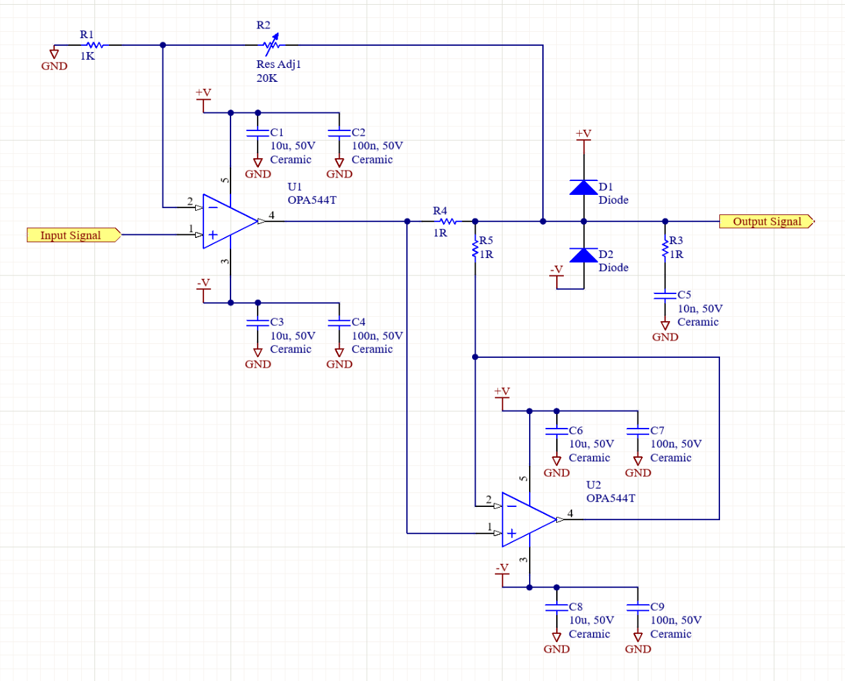
Figure 3: Two op-amp configuration for load sharing.
Choosing components
With the circuit worked out we just need to choose components. For now everything will be through hole since it’s being built on a bread board. The list of components is based on the two op-amp configuration since that includes all components for other configurations.
| Component | Name | Quantity | Digikey P# |
|---|---|---|---|
| U1, U2 | OPA544 | 2 | 296-15905-1-ND |
| DDPAK breakout | 2 | PA0185-ND | |
| Heat Sink | 2 | ||
| R3, R4, R5 | 1 Ohm, 2W | 3 | 13-FMP300FRF73-1RTR-ND |
| R2 | 20K pot | 1 | 3352W-1-203LF |
| R1 | 1K | 1 | Jelly bean |
| C1, C3, C6, C8 | 10uF, 50V | 5 | 445-173297-1-ND |
| C2, C4, C7, C9 | 100n, 50V | 4 | BC1101TR-ND |
| C4 | 10n, 50V | 1 | 399-4148-ND |
| D1, D2 | Fast, High P | 2 | SB5100DITR-ND |
BoM Cost at time of writing ~$83CAD
Results
The circuit was built up on a bread board with a signal generator input and the inductor on the output. Initially the circuit previously shown in Figure 3 was built. As predicted the op amp quickly over heated and went into thermal shutdown when running the full 1A pk-pk. While the circuit runs fine for the first 10 seconds, it should be able to maintain the 1A output for up to a few hours at a time, therefore the double op amp circuit was built up on a bread board as shown in Figure 4 .
This circuit significantly improved on the single op amp design allowing operation for 30+ seconds before entering thermal shutdown. I tried using a larger heatsink however this had little effect, likely since the heatsinks are on top of the package where the thermal resistance is higher. Due to the short on-time of the circuit it is difficult to comment on the signal to noise ratio. For this particular application SNR doesn’t matter, but I’d like to use the same circuit as a general voltage source in the future so improving SNR as much as possible would be nice.
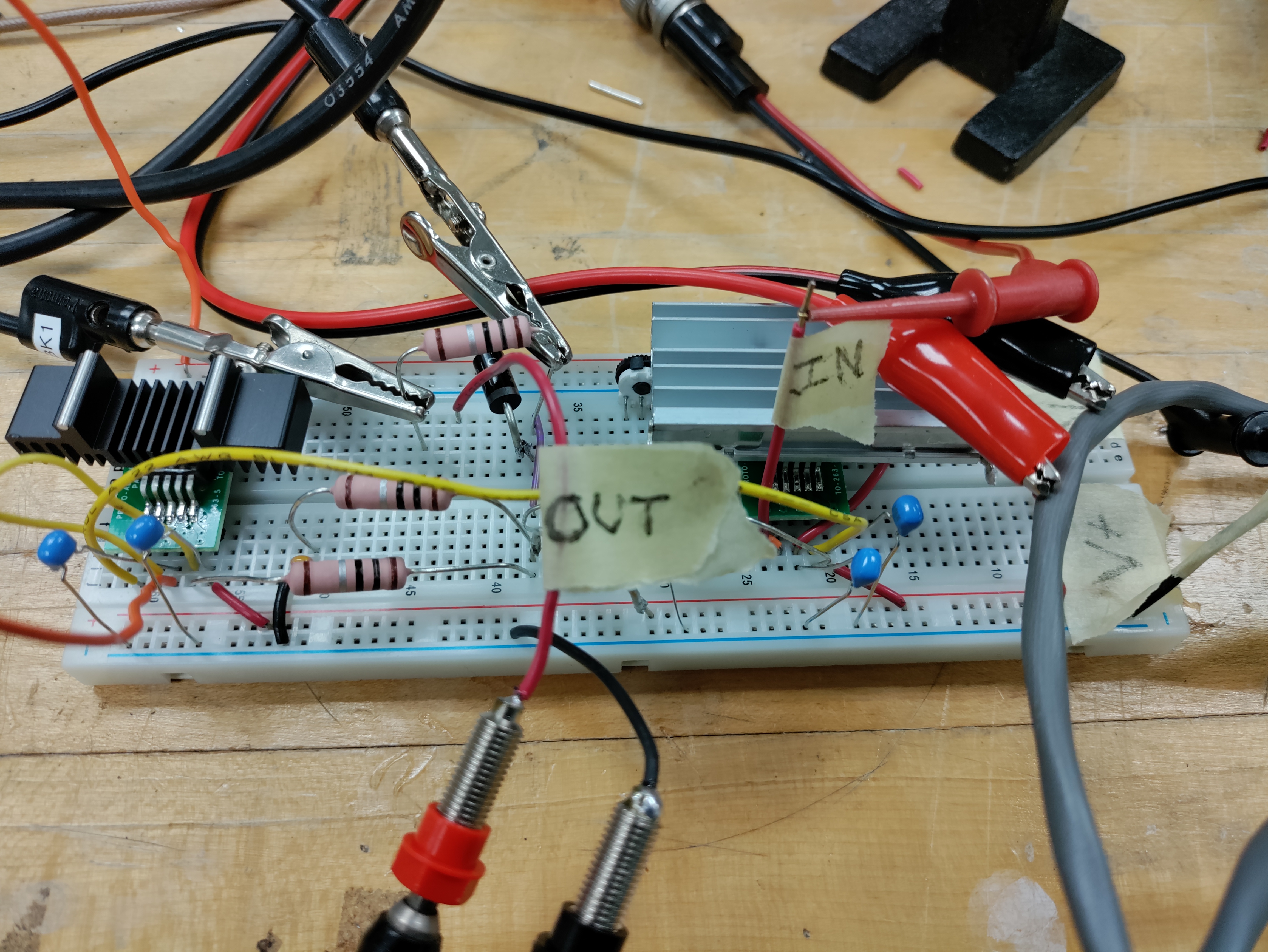
Figure 4: Dual Op Amp circuit set up on a bread board (in very messy fashion)
Due to the persistant issue of thermal throttling the time has come to design a PCB with even more op-amps to share the load and a well integrated thermal solution. This physical testing has left us in a good spot so the next post will be about the PCB design and final results!